

Low Energy Consumption on Post-Moore Platforms for HPC Research
Plataformas Post-Moore de Bajo Consumo Energético para la Investigación en HPC
ACI Avances en Ciencias e Ingenierías
Universidad San Francisco de Quito, Ecuador
Received: 02 December 2020
Accepted: 20 July 2021
Abstract: The increase in computational capacities has helped in the exploration, production and research process, allowing for the use of applications that were infeasible years ago. This increase has brought us into a new era (known as the Post-Moore Era) and produced a wide range of promising devices, such as Single Board Computers (SBC) and Personal Computers (PC) that can perform what could only be achieved on a server a decade ago. This work presents high performance computing devices with low monetary cost and low energy cost that meet the needs for the development of research in Artificial Intelligent (AI) applications, in-situ data analysis, and simulations that can be implemented on a large scale. These devices are compared in different tests, presenting advantages such as the performance per watt consumed, smart form, and more.
Keywords: Edge computing, embedded systems, manycore and heterogeneous computing, low-cost computing.
Resumen: El aumento de las capacidades computacionales ayudo en el proceso de exploración, producción e investigación, permitiendo la ejecución de aplicaciones que eran inviables hace algunos años. Este incremento de las prestaciones computacionales permitió el surgimiento de una nueva era conocida como era Post-Moore y produjo una amplia gama de dispositivos prometedores, como las tarjetas de placa única (SBC) y computadoras personales (PC) con rendimientos que solo se veían en un servidor hace una década. Este articulo presenta un análisis de dispositivos Post-Moore de bajo costo y consumo energético reducido que soportan despliegue y ejecución de aplicaciones para inteligencia artificial (AI), Análisis de datos in-situ y simulaciones que pueden implementarse en sistemas de gran escala. Estos dispositivos se comparan en diferentes pruebas, resaltando beneficios como el procesamiento por vatio consumido y escalabilidad.
Palabras clave: Computación Edge, Sistemas Embebidos, Computación Multinúcleo y Heterogénea, Computación de Bajo Costo.
INTRODUCTION
Two of the largest projects in Latin America have been the Fénix [1] supercomputer and the Santos Dumont Hybrid [2] supercomputer, both of which were manufactured by Atos. Fénix was commissioned by Petróleo Brasileiro S.A. [1] to be used in the oil and gas industry, while the Santos Dumont was built for the Laboratório Nacional de Computado Científica [2] for the academic segment and meets in the post 476 of the TOP500 list [3]. Fénix is among the top three on the continent and, at number 195 on the TOP500 list, provides a theoretical capacity of 4,297.42 TFlop/s and has a Linpack result of 1,836 TFlop/s with a consumption of approximately 287 kW. These capabilities have contributed to geophysical data processing using complex algorithms to generate images that are essential in oil exploration and production processes. With these computational capabilities, it will be possible to provide higher resolution images which will reduce operational and geological risks directly impacting the profitability of projects. The Fénix project demonstrates the great benefit of investing in technological tools, however, developing countries cannot always make those investments. Therefore, it is necessary to search for alternatives that can offer decent computing capabilities that also provide a good cost/benefit ratio.
Hardware has advanced in a complicated and long process, that has yielded beneficial results, the exponential increase of performance. Moore's law [4] was the guide for planning, development and investigation for decades. Numerous advances have arisen under its implementation. This triggered an improvement in performance thousands of millions of times. However, Moore’s Law has several limitations in practice and doesn’t always follow the exponential pattern. In 2016, the roadmap for semiconductor technology stopped focusing on "Moore's law", and its (complete) discontinuation is expected for the period 2025-2030 [5]. This change illustrates how application needs drive the advancement of technology. This has led to an "explosion" [6] of astonishing(impressive) computing capabilities. Algorithms that were previously inviable (Artificial Intelligence, Autonomous and deep learning) are at the top of current research and generate the technological evolution of countries. There is also an abundance of hardware with high computing capacity, low power consumption, and at an affordable price.
This paper focuses on the energy efficiency of low-cost devices and the different techniques and tools such as commands, monitors, hardware, and benchmark suites that can help with related issues. The first topic to be discussed will be the context in which computing is currently situated, followed by an explanation of reference devices, techniques and tools, and finally, a presentation of the results obtained from the tests performed
POST-MOORE ERA
Any attempt to overcome the limitations presented by Moore's law can be considered post-Moore [5]. Moore's law says that approximately every two years, the number of transistors in a microprocessor will double. In addition to this, the expansion is characterized by an increase in the clock frequency and a decrease in lithography [5], but limitations, such as size the lithography or quality of silicon, have caused Moore's law to begin to falter. This shift has generated new research paths such as multicores and heterogeneous computing. Furthermore, these emerging architectures do not focus on a single chip but on the combination of multiple chips [5]. This allows these architectures to adapt to the needs of each application, generating a sudden appearance and rapid diversification of the hardware. In order to achieve this integration, strategies such as Heterogeneous System Architecture (HSA), languages such as CUDA [14], OpenCL [15] or OpenACC [16], unification of CPU, GPU, FPGA, NPU, non-volatile 3D memory, reconfigurable communication grids, inductive wireless couplings, among others in a SoC [6, 7, 8, 9], must be taken into account.
As discussed above, the investment in computing resources is helpful for research and the development of countries, but developing countries often do not prioritize such things, which creates shortages in resources for computation. To reduce research costs, low-cost devices such as the Single Board Computer (SBC) or computer equipment heterogeneous desktop (PC) that can meet the needs of the applications can be made or bought. In addition, the applications must be developed or transcribed with the objective of being implemented in these architectures as a test base and these applications must maintain a portability and scalability that allows them the flexibility of deployment on architectures with greater capabilities. To verify the performance of different architectures, two reference devices are chosen that classify under the characteristics proposed by the Post-Moore Era. These devices will be addressed in the next section.
REFERENCE DEVICES
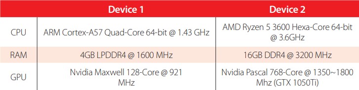
In order to compare performance, various devices were chosen to perform the experiments and compare the results. After several searches, there were several candidates, among which the following stand out: Raspberry Pi [17], Orange Pi [18], Asus Tinker Board [19], Odroid [20] and NVIDIA Jetson [21]. Of all these proposals, the NVIDIA Jetson family proved the best. The “Jetsons” are SBCs developed by Nvidia and in this group there are boards such as TK1 [22], TX2 [23] and Xavier [24]. Although their costs can be high and some production was suspended, from this family, Jetson Nano was chosen.
The Nano features provide us with an ARM CPU, a Nvidia GPU. The other architecture chosen has an AMD Ryzen CPU [25] and a Nvidia GPU, and is a somewhat more traditional architecture. The components that the experiments will focus on are the CPU and GPU, a review of which is provided in the following sections.
The CPUs
ARM Cortex-A57 is primarily composed of a finder, decoder instruction dispatcher, integer executor, load / storage unit (L1) and L2 memory system. It also has a floatingpoint unit, advanced SIMD, generic CPU interrupt control interface, generic timer, debug and trace.
AMD Ryzen 5 3600 is manufactured in a AMD Zen 2 microarchitecture. This design is given around small 8-core chiplets separated into 2 groups of 4. This allows the cores to be organized in a "central complex” or CCX, which contains the 4 cores and an L3 cache set. Regardless of the number of chiplets, it is paired with a central I/O via Infinity Fabric. This I/O acts as a central hub for all off-chip communications, as it houses all PCIe lanes, memory channels, and Infinity Fabric links to other chiplets or CPUs. This separation greatly improves its scalability and manufacturing capabilities as well as making it easier to build processors with many cores.
The GPUs
The selected GPUs are from successive architectures, NVIDIA Maxwell [26] and NVIDIA Pascal [27].
NVIDIA Maxwell focused primarily on energy efficiency and its SM (Streaming Multiprocessor) was restructured, partitioned and renamed SMM. The structure of the warp scheduler, along with the FP64 CUDA core and texture unit was inherited from NVIDIA Kepler [28], but the design of most execution units was partitioned so that each warp scheduler in an SMM handles a 32-core FP32 CUDA package. This enables better resource management than Kepler, saving more energy when the workload is not optimal for sharing resources. Maxwell would be succeeded by the Pascal microarchitecture.
NVIDIA Pascal architecture improvements are based on five technological advancements, 1) a 16nm fabrication process that increases performance and improves energy efficiency, 2) increased double precision performance for HPC workloads (in Deep Learning offers more than 12 times of neural network training and a 7-fold increase in Deep Learning inference performance compared to previous generation GPU architectures), 3) it is the first architecture to integrate revolutionary NVIDIA NVLink™ [29] bidirectional interconnect High Speed (this technology is designed to scale applications across multiple GPUs, delivering faster 5X acceleration of interconnect band), 4) using an innovative approach to memory design, CoWoS® (Chip-on-Wafer -onSubstrate) with HBM2 gives you a 3X boost in memory bandwidth performance over NVIDIA Maxwell ™ architecture, 5) the new in 16-bit medium-precision floating point instructions and the new 8-bit integer instructions allow AI algorithms to provide real-time responsiveness for Deep Learning inference.
These descriptions provide an idea of the specifications that these devices offer. In the next section, an explanation is given of the techniques and tools used to measure performance in the reference devices.
TECHNIQUES AND TOOLS
As shown in the introduction, computational capacities are immense and this requires large amounts of funds and investments and as such, the reference devices used in this study cannot be compared with the devices exposed in the introduction. Based on the Post-Moore approach, more affordable participants can be chosen. In order to simplify the choice, these devices should have at least one CPU and one GPU, it should also be possible to measure their power consumption. In this way, its capabilities can be verified by means of benchmarks.
There are many benchmark tools, from the reliable Linpack (HPL) [10] to Phoronix Test Suite (PTS) [11]. Energy consumption, hardware or other measurement variants can be used to obtain this data in a controlled way.
Benchmarks
Stress-ng [12] will test a computer system in various selectable ways. It can execute a wide range of CPU-specific stress tests that exercise floating point, integer, bit manipulation and control flow. It was designed to show thermal problems and errors in the operating system. Warning, if stress-ng was configured wrong, it may physically damage the device.
HPL (High-Performance Linpack) [10] solves a random dense linear system in double precision (64 bits) arithmetic on distributed-memory computers. HPL provides a testing and timing program to quantify the accuracy of the obtained solution, as well as the time it took to compute it. The generic implementations of MPI, the BLAS and VSIPL are available for a large variety of systems.
PTS (Phoronix Test Suite) [11] is a testing and evaluation platform. The software is designed to effectively carry out qualitative and quantitative benchmarks in a clean, reproducible, and user-friendly way. It will take care of the entire testing process, from dependency management to test download/installation, execution and aggregation of results. PTS has access to more than 100 tests used in the benchmark suite find in [13]. If there is a test that is not currently covered in PTS, it can be added through its extendable architecture.
Measure Power Consumption
As for measuring the power consumption, the aim is to generate the least possible load on the chosen devices, therefore, a measurement tool external to the device is chosen, which will measure the consumption second by second. For this task, we chose a smart outlet of the VTA brand.
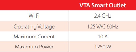
Specifications of the Measure Power Consumption.
The smart outlet counts a mobile APP, which carries a monthly history consumption, but video of second-by-second consumption can be taken when testing is performed. The devices are thought to have the lowest possible cost and decent capacities; therefore, SBCs are the best option that can be found, followed by Personal Computers (PC). Although their cost is not comparable to SBCs, they have higher power.
An SBC is a computer (CPU, RAM, GPU, etc.) on a single circuit or board. Its applications range from industrial environments to home IoT systems. Due to their high component integration and small footprint, these devices feature a higher reliability, better power handling, less weight and an SBC can be mass-produced to reduce its costs.
On the other hand, the PC has been heterogeneous for quite some time. In addition, over time, the cost of calculations per second has been decreasing, improving access to new hardware with greater power, allowing the development and implementation of countless applications. To measure the performance of each reference device, several tests must be carried out, the process of carrying out these tests is presented in the following section.
EXPERIMENTS
The tests perform two branches of experiments to measure the behavior of the chosen devices. The first branch focuses on the use of the CPU, the second on the use of the GPU. For CPU testing, Stress-ng and HPL were nominated. Stress-ng offers a variety of tests such as operations with floating numbers, integers, random numbers, matrices, among others. Bogo operations are the number of iterations of the stress test during the race. This is the metric for how much overall "work" has been accomplished in stress operations. The following configuration is used for this test:
stress-ng --cpu N --cpu-load P --cpu-method method --metrics-brief --timeout T
Where,
-- cpu N starts N jobs by stressing the CPU.
-- cpu-load P loads the CPU with a percentage P of load for stress jobs on the CPU. Accuracy depends on overall processor load and planner responsiveness, so the actual load may be different from the desired load. Also, the number of bogo operations may not scale linearly with load, as some systems employ CPU frequency scaling, and therefore heavier loads result in higher CPU frequency and higher bogo operations.
-- metrics-brief enables metrics and only shows non-zero metrics.
-- timeout T stops the stress test after T seconds. You can also specify units of time in seconds, minutes, hours, days, or years with the suffix s, m, h, d, or y.
-- cpu-method method specifies a CPU stress method. By default, all stress methods are exercised sequentially, however, only one method can be specified to use if necessary. Some methods were selected to measure the behavior of the CPU:
cfloat are 1000 iterations of a combination of complex floating-point operations.
correlate makes a correlation of random doubles: 16384 x 1024.
union performs integer arithmetic on a combination of bit fields in a C union. This shows how well (the compiler and the CPU) can perform loading and storing of integer bit fields.
hyperbolic calculates sinh(0) x cosh(0) + sinh(20) + cosh(30) for hyperbolic sine and cosine functions on float, double and long double, where 0 = 0 a 2n in 1500 steps.
prime finds all prime numbers in the range 1 to 1,000,000 using a slightly optimized brute force search.
matrixprod is a matrix product of two 128 x 128 double floating matrices. Testing in hardware shows that this provides a good combination of memory, cache, and floating-point operations and is probably the best method of measuring CPU performance.
In addition to the Stress-ng tests, HPL tests are performed. HPL is software that solves a dense, random linear system with double-precision (64-bit) arithmetic on computers with distributed memory. For the HPL test, it is configured as presented in the Table 3:
| Device | N | Parameter NB P | Q | ||
| Test 1 | Jetson Nano PC | 11584 23168 | 64 64 | 1 1 | 4 4 |
| Test 2 | Jetson Nano PC | 17376 34752 | 96 96 | 1 1 | 4 4 |
Configuring the HPL parameters.
In Test 1, the HPL.dat was configured to use ± 50% of the RAM capacity. Test 2 only uses 75% of the total capacity. It was configured in this way to take advantage of the capabilities that each device offered.
The next branch contains GPU usage tests, which are carried out with different tests that use OpenGL and CUDA, among others. The tests consist of building a terrain in a random way, simulating a colloid in a liquid medium and the CUDA nbody test, and using the PTS as a benchmark tool for this test. The tests are performed at 1080p for the Simulation-Visualization cases and with the power limiters disabled for all the tests.
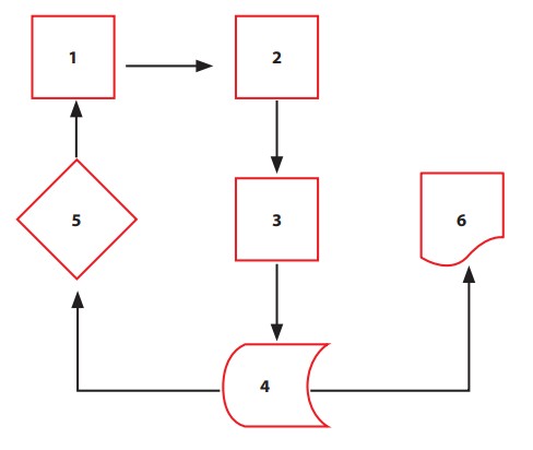
In order to better explain the tests, the Diagram of General Test Workflow is presented (Fig. 1). This diagram presents six steps and is described below:
Set up the different test requirements
As explained earlier in this section, each test is different and can modify values such as the duration time or the percentage of the test load. In addition, a test can modify the OS configuration files to increase the Hertz or the models of consumption of the devices. For these reasons, it is necessary to configure the test.
Configure the energy consumption monitor
The consumption monitor is always active and presenting data, therefore, after configuring the test, we must find a way to capture the data at the time of the test. If possible, one should look for monitors that keep a record of their measurements. If it is not possible, one can capture the behavior of the monitor during the test on video or by hand.
Start energy monitoring and launch test
Once the test is configured and it is ready to capture the data from the monitor, the test is run. An awareness ofthe beginning and end ofthe test is particularly important since this is when the probability of failure is highest.
Store and label test results
Labeling is an incredibly important step. When it is done incorrectly, it results in confusion when comparing the results of each device and the test may have to be repeated. If possible, the label should bear the name of the device, the test carried out, % ofworkload, and its duration or the consumption model.
Repeat the test to average the results or start a new test
In certain cases, it is necessary to have greater certainty in the results, therefore it is good to repeat the test several times and vary its configuration. This allows us to see patterns of behavior in the devices. The test can also be changed and these modifications can reveal problems like the thermal bottle, collars, memory saturation, or poor performance when loading or storing data types, etc.
Group the results and generate the graphs of the tests
Based on the labels, the data is processed to generate the graphs. For this document, the number of operations (Ops) per second performed was taken together with the number of watts to generate the Ops/W.
With this description, the following section shows the results obtained in each of the tests carried out for the different configurations.
RESULTS
In the previous section, the tests carried out for the analysis of the two reference devices were explained. It should be clarified that the ARM Cortex-A57 is presented with the A57 label, the AMD Ryzen 3600 uses the 3600 labels. As for GPUs, the tag used for the GPU of the Jetson Nano is Nano and the NVIDIA GP107 tag is used for the NVIDIA GTX 1050ti. Each test is performed five times per core (5 x 1 core, 5 x 2 core, etc.) and the results presented are the average of the values obtained in each test. The first tests to be performed are those carried out on the CPU. The first test performed is Cfloat, the unit of measurement will be Operations per watt (Ops/W), and, as indicated above, Cfloat is 1000 iterations of a combination of complex floating-point operations. The completion of these 1000 iterations is counted as an Operation (Ops) and the following graph (Fig. 2) shows the results of this test:
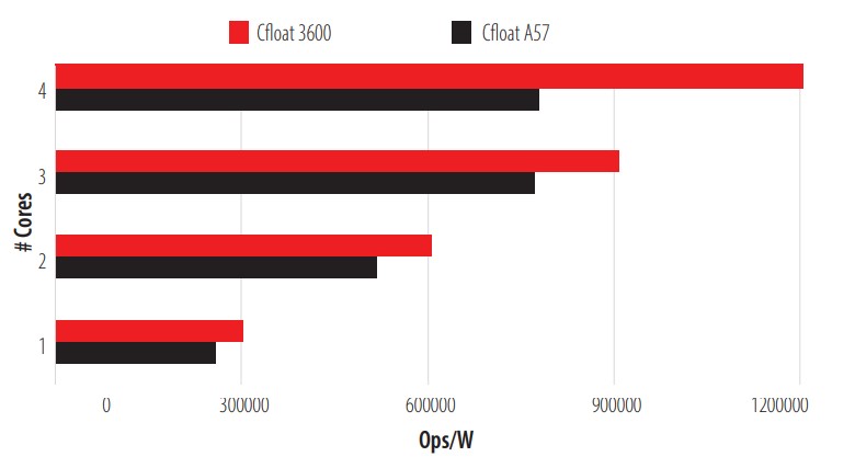
Cfloat test on CPU.
As shown in Figure 2, the 3600 has superior performance and better scalability in this test than the A57. It should be noted that the A57 suffers from a bottleneck when using all of its processors for the task, which flattens out scalability growth. The second test run is Correlation, an Ops consisting of the performance of a random double correlation (16384 x 1024), the results of which can be found in Fig. 3.
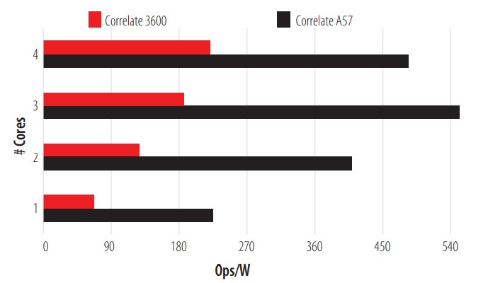
CPU Correlation Test.
In this test, the A57 stands out notably in its performance, but it is still affected by the bottleneck. Even so, it almost triples the performance of the 3600. The third test is a union test; the results are shown in Fig. 4.
The A57 shows an excellent handling (Compiler-CPU) of the loading and storage of bit fields, which is the strength of this test, almost quadrupling the performance of the 3600. The fourth test carried out was a hyperbolic test. It calculates hyperbolic sine and cosine functions with 1500 steps in each Ops, Fig. 5 shows these results.
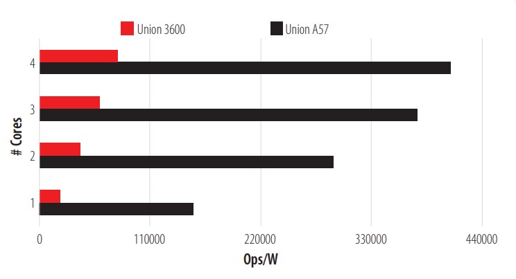
CPU Union test.
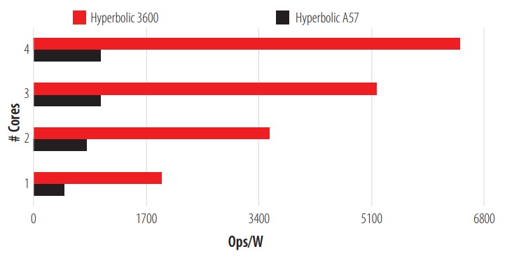
CPU Hyperbolic Test.
The 3600 showed excellent performance for this test, doing well in hyperbolic operations with float, double and long double, almost five times more than the A57. The fifth test is a calculation of the primes between 1 and 1,000,000. This calculation is carried out by means of brute force and once it is finished, it compares the results. If the results coincide, it is marked as an Ops. The results are presented in Fig. 6.
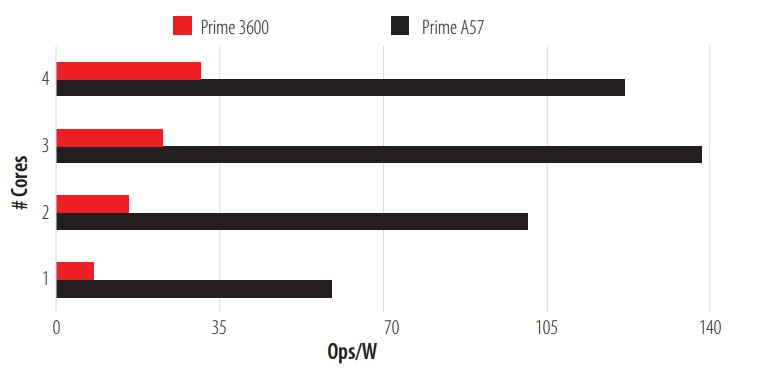
CPU Prime Test.
In this test, the A57 gives us superior performance per watt used, making it a good candidate for brute force tasks. The penultimate test performed is a multiplication of two 128x128 matrices. Each element in the matrix is in a double precision floating point format and once the task is completed, it is marked as an Ops. The results of this test can be seen in Fig. 7.
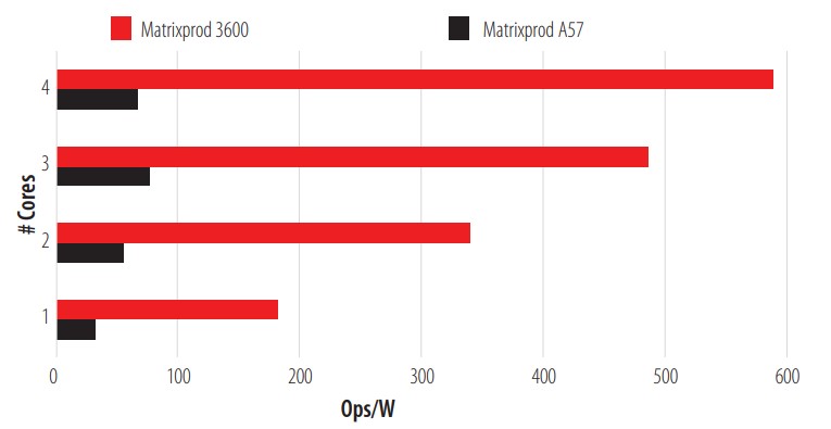
CPU Matrix Multiplication Test.
The results shown by the 3600 overwhelm the A57. With this preliminary matrix multiplication test completed, we move on to the next and last test, the HPL. HPL is one of the best-known benchmarks to test the performance of a CPU. Figure 8 shows the results.
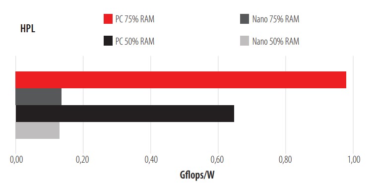
HPL for CPU.
The test was performed with two different loads and was done conservatively so as not to have the losses presented in the previous tests. As shown, the CPU 3600 achieves a performance of almost one Gflop per Watt consumed. After completing the task, the 3600 has consumed almost 8 Watts while the A57 has consumed about 7 Watts. The CPU 3600 provides a greater computational force than the A57 but it should be noted that the AMD Ryzen 3600 works at a frequency of 3.6 Ghz, while the ARM Cortex-A57 works at a frequency of 1.4 Ghz, among other differences.
The previous tests were carried out on the CPU and the following round of tests was carried out on the GPUs of the chosen devices. The GPUs are the GPU of the Jetson Nano (Nano) and the GTX 1050ti (GP107), Fig. 9, 10, and 11 present the results. Terrain (Figure 9) is a simulation of a field that is generated randomly. This generation is measured by frames per second (FPS). During this test, the ratio of FPS per Watt consumed during the task is shown and clearly, the Jetson Nano is far superior to that of the GTX 1050Ti (GP107).
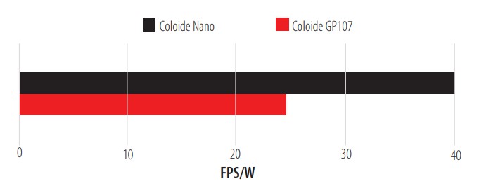
Colloid Simulation Tests.
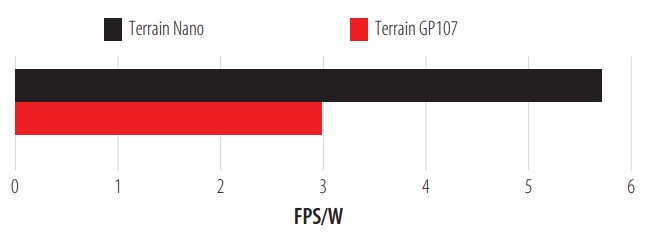
Terrain Simulation Test.
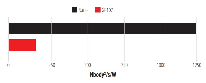
N-body test.
The Colloid test has the same configuration as Terrain and presents its result in the same unit of measurement, Fig. 10 shows the results. Colloid, like Terrain, shows us an excellent FPS/W ratio, almost double the FPS per Watt consumed. In addition, these two simulations were performed at 1080p.
For the final test, a deployment of the Phoronix Test Suite tool is performed. This tool provides us with several benchmarks. Mini-Nbody was selected as the test benchmark and the result is shown in Fig. 11.
The Nbody per Watt consumed ratio is considerably better in the Jetson Nano. It should be noted that each of the tests was performed in the maximum consumption mode for the Jetson Nano. As for the GP107, the configuration given by the manufacturer Asus in its ROG Strix model is maintained. Once these tests are performed according to Figure 1, several conclusions are reached. In the final section, these, and other conclusions that this work has generated, are presented.
CONCLUSIONS
As discussed at the beginning of this paper, the objective of this work is to propose lowcost computational options that take advantage of the characteristics of Post-Moore Era devices to increase benefit / cost ratio. With the abundance of devices this era has brought forth, two devices were selected to perform the same tests. SBCs are devices that stand out for their low cost and PCs for their wide use in different fields. Both offer computational capabilities that, less than a decade ago, were only found in servers or supercomputers. The investment in these devices is, in most cases, less than 5 ~ 10% of what it would be to invest in equipment for HPC.
The results presented in the previous section show that SBCs like the Jetson Nano are a great option for use as the computational force of an investigation. These devices provide researchers with computational strength on par with more traditional options. Due to its shape, we can take advantage of its energy efficiency to be implemented in different tasks and environments.
Both SBCs and PCs are excellent options from an economic point of view to encourage investment in research and development. The current PC offers us considerable computational strength at affordable prices, while SBCs provide the advantage of low energy consumption. Both options can be implemented in multiple tasks, achieving great performance.
In addition to this, the specifications of these devices make them essential for the development of applications designed to be scalable, portable, simple and efficient. Because, when developing an application for these devices, tests can be carried out with different amounts of data or be deployed on different platforms, more flexibility is available to applications when implemented on servers or supercomputers.
FURTHER WORK
The most intense tests were performed on the CPU. For future work, a series of easy-to- implement, high computational effort tests will be developed on the GPU. In the first instance, the tests are written in CUDA, then transcribed into other languages. Once this stage is complete, an implementation methodology will be proposed to measure the impact on performance when testing is performed non-natively (using methods such as containers).
AUTHOR CONTRIBUTIONS
The authors contributed as follows: the first author Pablo Josue Rojas Yepes carried out Investigation, Methodology, Visualization, Writing - original draft. The second author Carlos Jaime Barrios Hernandez carried out Funding acquisition, Project administration, Resources, Supervision, Writing - review & editing. The third author Luiz Angelo Steffenel performed Project administration, Supervision, Writing - review & editing.
CONFLICT OF INTEREST
The authors do not present any conflict of interest with the work performed.
REFERENCES
The T0P500 List. Fénix, (02, 2020). SYS-1029GQ-TRT, https://www.top500.org/system/179681, last accessed 2020/2/20.
The T0P500 List, (02, 2020). Santos Dumont Hybrid - Bullx B710, https://www.top500.org/system/178569, last accessed.
The T0P500 List, (06, 2020), https://www.top500.org/lists/top500/2020/06/, last accessed.
M. Waldrop., (s.f.). The chips are down for Moore's law. Nature. 530 (7589): 144-147. DOI: http://dx.doi.org/10.1038/530144aISSN0028-0836. PMID 26863965.
S. Matsuoka et al., (s.f.). From FLOPS to BYTES: Disruptive change in High-Performance Computing towards the Post-Moore Era. In CF '16 Proceedings of the ACM International Conference on Computing Frontiers. 2016-05-16. ACM New York, NY, USA. DOI: http://dx.doi.org/10.1145/2903150.2906830
S. Matsuoka., (s.f.). Cambrian explosion of computing and big data in the Post-Moore era. In HPDC '18 Proceedings of the 27th International Symposium on High-Performance Parallel and Distributed Computing. 2018-06-11. ACM New York, NY, USA. DOI: https://doi.org/10.1145/3208040.3225055
K. Barker et al., (2005). On the feasibility of optical circuit switching for high performance computing systems. In Proc. of IEEE/ACM SC 2005, pages 16-16.
Take, Y., Matsutani, H., Sasaki, H., Koibuchi, M., Kuroda, T. and Amano. H., (2014). 3D noc with inductive- couplings for building-block SiPs. In IEEE Trans. on Computers, pages 748-763. 63 (3).
Kagami, T., Matsutani, H., Koibuchi, M., Take, Y., Kuroda, T. and Amano, H., (02, 2016). Efficient 3-D bus architectures for inductive-coupling ThruChip Interfaces. In IEEE Trans. on VLSI systems, pages 493-506. Vol.24, No.2.
Inadomi, Y., Patki, T., Inoue, K., Aoyagi, M., Rountree, R., Schulz, M., Lowenthal, D., Wada, Y., Fukazawa, K., Ueda, M., Kondo, M., and Miyoshi, I., (2015). Analyzing and mitigating the impact of manufacturing variability in power-constrained supercomputing. In Proc. of IEEE/ACM SC15.
HPL- A Portable Implementation of the High-Performance Linpack Benchmark for Distributed-Memory Computers, (02, 2020). https://www.netlib.org/benchmark/hpl/
Phoronix Test Suite, (02, 2020). https://www.phoronix-test-suite.com/, last accessed.
Stress-ng, (02, 2020). https://wiki.ubuntu.com/Kernel/Reference/stress-ng, last accessed.
Open benchmarking, (02, 2020). https://openbenchmarking.org/, last accessed.
Nvidia, CUDA, (03, 2020), https://docs.nvidia.com/cuda/index.html last accessed.
Kronos Group, OpenCL, (03, 2020), https://www.khronos.org/about/ last accessed.
OpenACC, (03, 2020), https://www.openacc.org/resources last accessed.
Raspberry Foundation, Raspberry pi, (04, 2020), https://www.raspberrypi.org/products/, last accessed.
Orange pi, (04, 2020), http://www.orangepi.org/ last accessed.
Asus, Asus Tinker Board, (04,2020), https://tinker-board.asus.com/product/tinker-board.html last accessed.
Hardkernel, Odroid, (04,2020), https://wiki.odroid.com/, last accessed.
Nvidia Developer, Sistemas Integrados Avanzados para la Computación en el Edge, (04, 2020), https://www.nvidia.com/es-la/autonomous-machines/embedded-systems/, last accessed.
Nvidia Developer, Jetson TK1, (04,2020), https://developer.nvidia.com/embedded/jetson-tk1-developer-kit, last accessed.
Nvidia Developer, Jetson TX2, (04, 2020), https://www.nvidia.com/es-la/autonomous-machines/embedded-systems/jetson-tx2/, last accessed.
Nvidia Developer, Jetson Xavier NX, (04, 2020), https://www.nvidia.com/es-la/autonomous-machines/embedded-systems/jetson-xavier-nx/, last accessed.