

Design of low-voltage low-power CMOS current reference in 180nm
Diseño de un espejo de corriente CMOS a baja potencia y voltaje en 180nm
ACI Avances en Ciencias e Ingenierías
Universidad San Francisco de Quito, Ecuador
Received: 14 May 2019
Accepted: 27 November 2019
Resumen: Este artículo muestra las mejoras de diseño para un espejo de corriente o current referenceoriginalmente basado en un espejo de corriente con voltaje dual de umbral en dos etapas, dichas etapas han sido modificadas para mejorar tanto la dependencia de corriente para una configuración en modo diodo de un transistor así como las figuras de mérito, ambas cualidades son comparadas con el circuito base. La presente solución ha sido diseñada sobre tecnología CMOS TSMC en 0.18 μm y analizada a través de la simulación del circuito en Virtuoso de Cadence. Los resultados de las simulaciones muestran que cuando el voltaje del substrato es polarizado se tiene una corriente en salida de 342 nA y una potencia de consumo por debajo de los 513 nW con un voltaje de operación máximo de 1.5 V a temperatura ambiente. La sensibilidad lineal es 1 %/V, mientras que el coeficiente de temperatura es 17 ppm/°C. Por otro lado, cuando la polarización del substrato es omitida, es decir el substrato conectado a la fuente del transistor, el circuito muestra una corriente en salida de 188 nA y una potencia de consumo por debajo de 282 nW con un voltaje de operación máximo de 1.5 V a temperatura ambiente, La sensibilidad lineal es 2.89 %/V, mientras que el coeficiente de temperatura es 23 ppm/°C. El documento está compuesto de cuatro secciones, la primera sección muestra el estado de arte acerca de los espejos de corriente para un bajo consumo. La segunda sección muestra los métodos para implementar los cuatro diferentes diseños, como son el dimensionamiento y los parámetros eléctricos de las fuentes de alimentación. La tercera sección muestra los resultados obtenidos en cada uno de los circuitos y una comparativa de las figuras de mérito calculadas. Finalmente, la cuarta sección muestra las conclusiones de cada bloque, los beneficios obtenidos al implementar cada uno de los diseños así como la mejor solución acorde a las figuras de merito obtenidas.
Palabras clave: espejo corriente, CMOS, inversión débil, MOSFET, consumo, potencia, coeficiente temperatura, sensibilidad carga.
Abstract: This paper describes design improvement of a current reference, originally based on dual-threshold voltage current mirror stages, these stages have been modified in order to improve the temperature dependence of the current of a diode-connected transistor and the figures of merit (FOM), both of them compared to the base-circuit. The proposed solution has been designed in a 0.18 μm CMOS TSMC technology and analyzed through circuit simulation. Simulation results, when a body-bias generator is used, show an output current of 342 nA and a power consumption below 513 nW at the maximum operating voltage of 1.5 V and at room temperature. The linear sensitivity is 1%/V, while the temperature coefficient is 17 ppm/°C. On the other hand, when the body-bias generator is neglected, the circuit shows an output current of 188 nA and a power consumption below 282 nW at the maximum operating voltage of 1.5 V and at room temperature. The linear sensitivity is 2.89%/V, while the temperature coefficient is 23 ppm/°C.
Keywords: current reference, low-voltage, low-power, CMOS, current mirror.
INTRODUCTION
The rapid growth of low power applications in fields like: Internet of Things (IoT), entertainment, biomedical, mobile networks and power control systems, is changing the lifestyle of the new generations, where the electronic devices are being used everyday life. However, the current control faces several challenges, such as temperature and power supply dependence. This paper presents a structure for designing a current reference circuit in low-voltage and power-consumption, which are the main arguments at the time of designing a current reference.
In response to the power scaling a wide quantity of topologies can be used where the bias point is the parameter to reach a better performance. One of these topologies is the peaking current mirror, where an increasing at the output current is due to a drop voltage over a resistance in order to drive the current [2]. Though, its dependency of resistances to work leads to an unsuitable option when the temperature dependence should be reduced since the final circuit is created by the addition of multiple current peaks until reaching the operational bias point [2]. The beta multiplier current reference whose resistor to bias the circuit in subthreshold operation is small, even for a value of current in nanoampere range, the drawback of this circuit is the needed of different voltages in order to bias the NMOS and PMOS transistors so the temperature and supply dependency can not be reached rapidly [4]. Other solution where the self-biased principle was used is a circuit where the temperature is compensated by gate-leakage transistors, these are biased by a reference voltage generated for a self-regulated 4T push pull circuit; in this case, occupancy area could be a problem at the design time [3]. Another solution where the self-biased principle is used, is the 3T CMOS current reference, where the circuit is composed by two stages. The first is a reference voltage where the temperature dependency is reduced and the second stage is composed by an active-load where the supply dependency is driven by the operational point reached in the previous stage [1].
METHODS
This paper shows an improvement for the 3T CMOS current reference showed in [1]. Fig. 1A shows the basic model for a current reference where the MH transistor must have a oxide thickness greater than the ML transistor in order to create a Vx as close as possible to the minimum-temperature-coefficient (MTC) point of the load transistor. Fig. 1B shows the block diagram representation of the improvement that was done in this paper. The main block represents the basic current reference where T1, T2 and T3 takes the place of ML, MH and load transistor from the 3T-design. The other block, composed by MA and MB represents a voltage reference circuit whose functions is biasing the bulk of the transistor in the blocks T2 and T3.
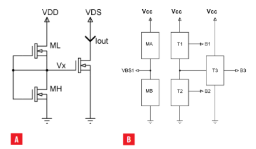
(A) 3T CMOS current reference model [1]. (B) Diagram block representation for this paper.
In function of the block diagram, four designs were implemented in this work to test different ways of designing a current reference with fixed requirements and the best response at the figure of merit. The first design shown in Fig. 2A where the T1 is composed by two transistors in series connection and T2 is composed by two transistor in diode-connected mode, while the active load has only one transistor. In this case, the body-bias generator was neglected. Fig. 2B shows a variation of the previous design in T1 and T3 block, T1-block presents a cascode connection between two transistors, in this case the variation of supply voltage is driven by the top transistor in T1 block and self-regulated since the gate is tied to the output voltage of the reference circuit, Vx. Moreover, T3 block presents a self-cascode connection between seven transistors to increase the effective length of the active load. Thus the possible current to control can be increased using the same MTC point.
Fig. 3A shows a design where an extra voltage reference is used to bias the bulk of the top transistor in block T2. This allows to change the threshold voltage of the transistor and to reduce the power consumption during the transistor working in weak-inversion mode.
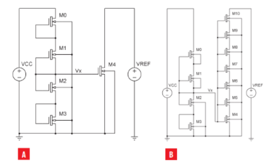
(A) Current reference with improvements in T1 and T2 block (B) Current reference with improvements in T1, T2 and T3 block
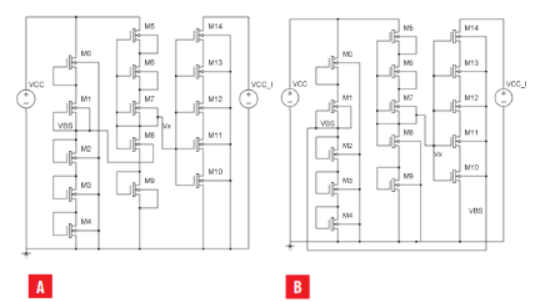
(A) Current reference with body-bias generator for T2 (B) Current reference with body-bias generator for T3 block
FINDINGS
The proposed current reference circuits were implemented in a 180nm TSMC CMOS technology. The circuit can operate by a supply voltage from 0.6V to 0.77V as VDDMIN. The IREF can achieve in the best case 177 nA and 10uA for the worst case. Furthermore, the cases wherethebody-bias generator wasused, these alwaysgivea nanoampereresponse whereas the first circuit presents larger power consumption in comparison to the other designs. The temperature coefficient in all the cases is always smaller than 50, the linear sensitivity is smaller than 5 and the best results are shown when the body-bias was used in the T2-block.
Fig. 4A shows the output current of all the designs. The first of them has the greater power consumption in micro-amperes since the active load was implemented only with one transistor, so its sizing was wider than the others designs. The best solution was reached in the second design, where the active load was implemented with seven transistors in self-cascode mode contemplating a better controlled transconductance and the channel length (which is the adding result of the length-transistor) that allows to reduce the power consumption by keeping the same gate-source voltage used to bias the active load.
Fig. 4B shows the output voltage from the voltage reference, the first path for the first and second design, and the second path for the third design. In this case the initial requirement, VREF ≈ 500 [mV], was reached by all designs. The minimum voltage for the power supply was reached at 0.6 V. Thus, if the initial requirement for the voltage reference is lower than the fixed in this paper, it will be possible to reduce the power supply.
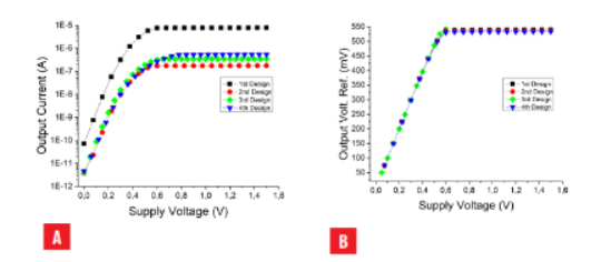
(A) Output current in function of the power supply variation (B) Output voltage reference in function of the power supply variation
Fig. 5A shows the linear sensitivity (LS) along the voltage supply variations, from 0.6 V to 1.5 V, where all designs exhibits a LS lower than 4%/V. The best solution is given by the designwhere the body-bias generator was used to provide voltage to the T2-Block, since higherbody-source voltage lower the reference voltage, i.e. MTC point. In the active load yields a slight variation at the output current so the linear sensitivity is reduced too. Vhen the bodybiasgenerator is used inT3-block, thereferencevoltage is notreduced while the bodyeffectin theactive load isreduced.Thisprovides animprovement at the outputcurrent.
Fig. 5B shows the temperature coefficient (TC) of the all designs. The first three implementations show a TC lower than 20 ppm/°C, the third implementation shows the worst result due to the output current reached at the minimum voltage supply. This latter value is slightly greater than 0.6 V, and the temperature variations can not be driven by the active load where the body-bias is working.
Fig. 6A shows the total power consumption of the implementations. The second circuit shows the better result in view of the active load driven by seven transistors in self- cascode connection and the channel length that allows a better driving output current. In addition to the current driving, the SC connection allows to reduce the power because the bias voltage to power the active load is lower than a simple transistor with same composite channel length.
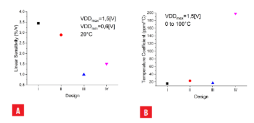
(A) Linear sensitivity results (B) Temperature coefficient results
Fig. 6B shows the power consumption of the voltage reference which work is to provide the reference, i.e. MTC point, to the active load. The best result is given by the design where the body-bias generator was used to bias the bulk of T2-block. For this reason, the path consumes less power due to a part of the power driven by the generator. In this path the power consumption is reduced because of the voltage reference sizing used to generate a body-bias voltage (VBS) that has a low value.
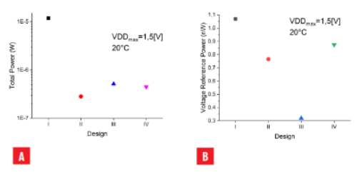
(A) Total power consumption (B) Voltage reference power consumption
The previous results can be improved if the design methodology follows the next steps:
T1 block can be implemented with different structures, shown in Fig. 2A - 2B, from a simple transistor, which works in subthreshold regime since Vth = 0, to a series- connected MOSFETs which body can either be connected to a bias voltage or ground point. This improvement allows to the body-source voltage becomes more negative so the VTH and T1 block conductivity is reduced.
Stacking thetransistors in theT2 block leads to amplifying thedifference of threshold voltages of the transistors used in the block T1 and T2.
The T3 block improvements used series-connected transistors to increase the effective channel length, i.e. A larger channel, a smaller load sensitivity of the circuit.
The body connection can be used as a key to control the threshold voltage when the transistor works in weak region, and consequently the temperature coefficient, the linear sensitivity and the minimum voltage supply can be improved.
e final implementation showed in Fig. 3A, has three self-biased transistors in stacking, M5− M7, in block T1, two transistors in diode-connected (gate to drain), M8 − M9 in block T2 andfive series-connected transistors, M10 − M14 for the block T3. In addition to these transistors,there are a body-bias circuit with five transistors, M0 − M4, to bias the upper transistor, M8,of block T2. This implementation shows all the possible cases where the circuit can becontrolled by the body connection. Hence, exploiting the transistor sizing, the designercan potentially use transistors of the same type in all the three main blocks T1, T2, and T3,therefore reducing significantly the process sensitivity of the current reference.
Table 1 shows the results for all designs in two cases where a trimming process wasimplemented. Thus, the performance of each design can be improved to the needs of thedesigner. The last two designs show an extra parameter which value is used to bias thesubstrate of the transistors, i.e. body-bias voltage VBS. The drawback of “VBS to T3-block”design is the increasing of the minimum voltage supply and the temperature coefficient.In contrast, the best result is given by “VBS to T2-block” in which temperature coefficientand linear sensitivity gives smaller values in the trade-off to the body-bias voltage.
| Design | ||||||||
| 1st Improv. | 2nd Improv. | VBS to T2-block | VBS to T3-block | |||||
| FOM | case I | case II | case I | case II | case I | case II | case I | case II |
| TC[ppm/°C] | 16 | 18 | 25 | 23 | 28 | 17 | 198 | 40 |
| LS[%/V] | 3.45 | 2.64 | 2.41 | 2.89 | 0.66 | 0.99 | 1.51 | 6.03 |
| VDDMIN [V] | 0.6 | 0.6 | 0.6 | 0.6 | 0.6 | 0.6 | 0.6 | 0.77 |
| VREF @20 C[V] | 0.54 | 0.52 | 0.524 | 0.535 | 0.528 | 0.564 | 0.533 | 0.691 |
| IREF@20 C[nA] | 7.85 | 10 | 176 | 188 | 263 | 342 | 298 | 534 |
| PS[%] | 3.73 | 2.34 | 2.18 | 2.63 | 1.94 | 7.87 | 1.36 | 3.81 |
| Total Power[V] | 11.77u | 15u | 263n | 282n | 394n | 513n | 447n | 801n |
| VBS@20 C[mV] | 62 | 55 | 50 | 106 | ||||
Figure of merit for all designs
CONCLUSIONS
In comparison to the 3T current reference showed in [1], these improvements need a greater occupancy area in trades-off the load sensitivity, process sensitivity and power consumption mainly.
The aim of T1 block is controlling the linear sensitivity, larger length channel and conductivity. Thus, leading to reduce the impact of VDD on Vx variations and consequently on IREF . It is worth noting, the body to the source connection is used to avoid the body effect.
The gate-drain connection was used to increase the threshold voltage in T2 block and consequently has a Vx more stable since a low VMTC guarantees a current reference with a low-voltage and low-power consumption. The number of transistors in block T2 is due to reach of Vx required.
The output current can be set with the number of transistors used to implement T3 block. A greater number of transistors, a smaller output current IREF .
If the body transistor load is biased with a voltage different to zero, the VMTC can be minimized, hence the Vx required is reduced too. The increase in the number of body connections in the circuit means a more difficult circuit to control and more occupancy area.
If the power consumption of the voltage reference and the linear sensitivity requirements are not relevant for the aim circuit for biasing, the design depicted in Fig. 2B can be used with some advantages. These advantages are: the circuit will use a smaller occupancy area, and the temperature coefficient should be lower than 20 ppm/°C and the linear sensitivity will be approximately 3%/V. In this manner, an output current dependency of the voltage supply is guaranteed.
The body-bias generator allows to reduce the temperature coefficient and linear sensitivity. However, the total power consumption is increased by more transistors and as a result, greater current to bias the entire circuit is needed.
AUTHORS’ CONTRIBUTION
Diego Jaramillo added the schematics for his simulation and analysis, in addition to the writing of the manuscript. Nanoelectronics Laboratory of the University of Calabria - DIMES, Italy tests the licenses for the Virtuoso Cadence software as well as the libraries for 180 nm technology from TSMC.
REFERENCES
[1] Crupi, F., Rose, R. D., Paliy, M., Lanuzza, M., Perna, M., & Iannaccone, G. (2017, dec). A portable class of 3-transistor current references with low-power sub-0.5 v operation. International Journal of Circuit Theory and Applications, 46 (4), 779 795. doi: https://doi.org/10.1002/cta.2439
[2] Hirano, M., Tsukiji, N., & Kobayashi, H. (2016, oct). Simple reference current source insensitive to power supply voltage variation improved minoru nagata current source. In 2016 13th IEEE international conference on solid-state and integrated circuit technology ICSICT. IEEE. doi: https://dx.doi.org/10.1109/icsict.2016.7998846
[3] Vang, H., & Mercier, P. P. (2016, may). A 14.5 pV, 31 ppm/ c resistor-less 5 pA current reference employing a self- regulated push-pull voltage reference generator. In 2016 IEEE international symposium on circuits and systems (ISCAS). IEEE. doi: https://dx.doi.org/10.1109/iscas.2016.7527484
[4] Yadav, C., & Prasad, S. (2017, aug). 20na sub-threshold biased CMOS reference current source. In 2017 international conference on information, communication, instrumentation and control (ICICIC). IEEE. doi: 10.1109/ icomicon.2017.8279144